Some time ago, Li Auto's paper mentioned that silicon carbide epitaxial defects will cause SiC MOSFETs to fail (click to view), which shows that it is very important to reduce epitaxial wafer defects.
May 21, Singapore A-STARInstitute of Microelectronics and FranceSOITEC published an article titled "SiC epitaxial wafers move towards defect-free".
The team said that currently commercially available 6-inch and 8-inch substrates can already be microtubule-free and have a low dislocation density: the base dislocation is less than 500 pieces/cm2, the threading dislocation and screw dislocation are less than 5000/cm2。 However, in order to prepare high-quality silicon carbide devices, silicon carbide epitaxy is still needed to optimize to further reduce defect density, especially "fatal defects".
The team has mainly achieved 2 major breakthroughs:
Carbon-plane SiC epitaxy
Defect density less than 0.1 pcs/cm2
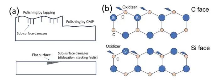
Due to the polarization of Si-C bonds, the top surface of SiC can exhibit 2Polarity: silicon surface or carbon surface, the two polarities have completely different surface characteristics and properties
Therefore, today's SiC high-power device technology mainly uses silicon-faced SiC substrates. This is because this surface ensures a high-quality interface and a large band offset from the gate oxide layer.
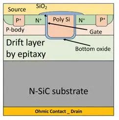
However, for trench-gate SiC MOSFETs, the carbon plane is more advantageous.
Because in a trench-gate SiC MOSFET, the gate stack of both silicon and carbon substrates is in SiC (113). formed on the surface.
Due to the fast oxidation rate of the carbon surface, it forms an oxide layer at the bottom of the trench twice as thick as the oxide layer on the sidewall, which simplifies the manufacturing process and increases the gate breakdown voltage. Although the band shift between SiO and carbon-plane SiC is small, these advantages are still objective.
Based on this, the team from A-STAR, the National University of Singapore and Soitec demonstrated a virtually defect-free carbon surface SiC epitaxial growth process with extremely high growth rates – SiC on the 6-inch carbon planeOn the substrate, the growth rate is about 50 μm/h.
According to the team, they first loaded an n-type carbon face into a commercial hot-wall CVD system SiC 150 mm substrate, then a buffer layer of about 0.5 μm thick was grown, followed by 50The growth rate of microns/hour was 11 μm thickSiC drift layer.
The thickness of the buffer layer and the drift layer was confirmed by Fourier transform infrared spectroscopy and the thickness uniformity was determined to be less than 3%. Atomic force microscopy tests showed that the epitaxial sheet had a smooth surface and a root mean square roughness of just below 0.3nm.
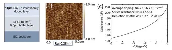
The doping distribution results showed that the unintentional (or background) doping in the carbon-plane SiC epitaxial layer was about1.5 x 1015cm-3This value can accurately control the drift layer doping of the SiC MOSFET device1-2 x 1016cm-3Range.
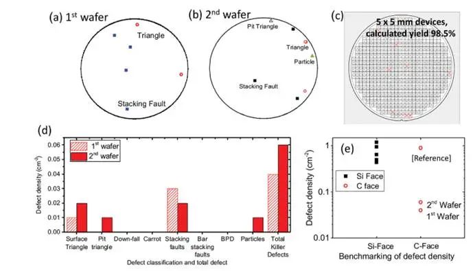
The defect density of carbon-plane SiC epitaxial wafers was measured using the KLA Candela 8520 system, and the results showed that: The epitaxial wafer has very low material defects – a defect density of less than 0.1/cm2。 Compared with silicon-faced SiC epitaxial layers, the defect density of carbon-faced SiC epitaxial wafers is almost an order of magnitude lower.
The team said this indicates that the silicon carbide epitaxial material produced by their growth process has few defects, 5×5mm2The device's yield of up to 98.5% provides significant advantages for carbon-plane SiC devices, especially in large-format device architectures such as bipolar devices.
The team analyzed that a key factor in their near-defect-free silicon carbide epitaxy was the significant reduction of surface and subsurface crystal defects present in SiC substrates upfront.
They do this by optimizing the chemical-mechanical polishing process, which involves oxidation and oxide removal, which is customized for carbon-faced SiC and has a much higher oxidation rate than the silicon side. By customizing the chemical-mechanical polishing process, they can produce smooth silicon carbide substrate surfaces with minimal subsurface damage.
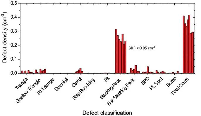
Typically, the most prominent defects in silicon carbide epitaxial processes are base dislocations and stack dislocations. To minimize these defects, most defect densities are around 500/cm2The base dislocation will be converted into a penetrating edge dislocation.
The team used an optimized hydrogen etching process to prevent the substrate dislocation from being converted into a more difficult Shockley stack dislocation. At the same time, the high growth rate of 50 μm/h also promotes the conversion of base dislocation to penetrating edge dislocation, which is further reducedBase plane dislocation in SiC epitaxial layers.
The team also said that another advantage of carbon-plane epitaxy is that it favors stepped flow growth because it has a long diffusion length – greater than 1μm. Because of this, combined with the high conversion rate of the substrate dislocation to the penetrating edge dislocation, they achieved virtually defect-free carbon-plane SiC epitaxy.
silicon-faced SiC epitaxyBasis dislocation defects less than 0.05/cm2
In addition to developing carbon-faced SiC wafer epitaxy processes, the team has also innovated the traditional silicon-faced SiC wafer epitaxy process and is in A breakthrough was achieved on an 8-inch silicon carbide substrate. The key to their success is to convert the substrate dislocation in the substrate into the through-edge dislocation in the buffer layer before the device drift layer grows.
The breakthrough in silicon-faced silicon carbide epitaxial process was based on the research of Tangali Sudarshan's team at the University of South Carolina in 2005They made it possible to remove the base dislocation by etching the substrate surface with potassium hydroxide before placing the silicon carbide substrate into the treatment chamber. However, the downside of this process is that it is not suitable for large-scale production of SiC epitaxy.
But this principle has many advantages, such as the preparation of silicon carbide substrate surfaces by etching around the base dislocation region to facilitate its conversion to penetrating edge dislocations during epitaxial growth.
Based on this method, the team developed an in-situ etching technique for SiC substrates that introduces two etching steps: one during baking and the other between the buffer layer growth steps. In-situ hydrogen etching at processing temperature, surface recovery through back-etching, and material recovery through low-temperature baking can effectively filter out substantial dislocations in the drift layer. The materials produced by this process are practical and scalable for SiC epitaxial manufacturing, achieving almost 100% base-free dislocation
KLA Candela 8520 test results show that a batch of eight pieces of < is <b11> SiC substrate in-situ etching technology/b20> The base dislocation of SiC substrates is almost eliminated, and the density is less than 0.05/cm2。
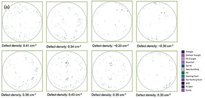
Another advantage of this process is the significant reduction in defect density, from the typical 1.0/cm2to just 0.3-0.4/cm2。